Tabletop SEM Products List (NEW)

Tabletop SEM (Scanning Electron Microscopes)

A scanning electron microscope (SEM) is a type of electron microscope that creates a high-resolution image by scanning the surface of a sample with a focused beam of electrons. SEMs generate images that provide details about a material’s surface composition and topography.

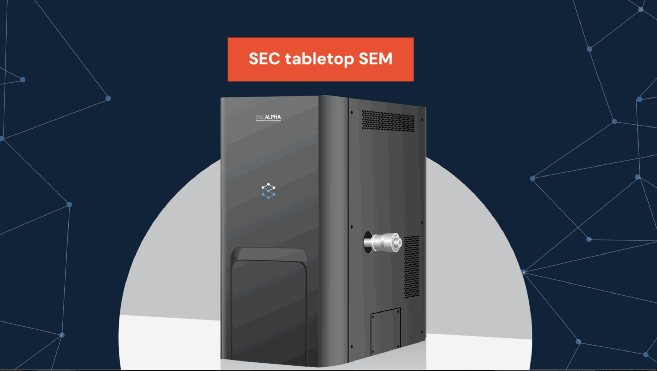
SNE-Alpha

SNE-Alpha

High Resolution Table Top SEM with 5-Axis XYZRT stage, 5nm Resolution, Variable Aperatures

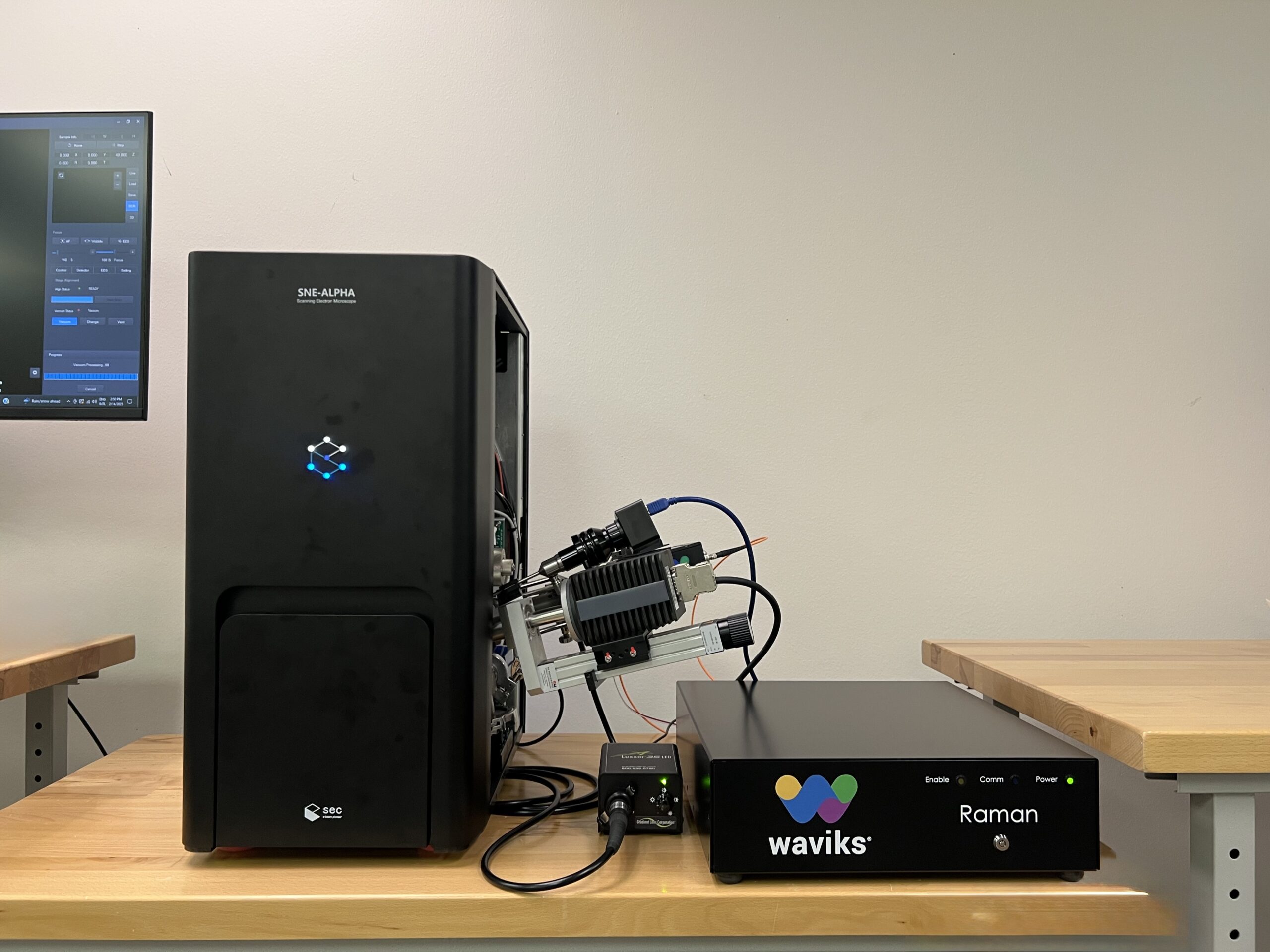
Accessories for Tabletop SEM

img3b

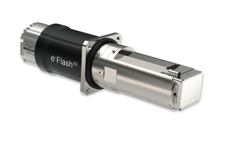
BRUKER XFLASH EDS

XFlash 360 for Tabletop SEM with 30mm2 SDD and Esprit Compact Software

Photo Aug 21 2020, 4 37 49 PM-2

EBIC

EBIC is an Analysis Technique Used Primarily in the SEM for Semiconductor and LED Research

CATHSCENCE

Cathodoluminescence

img4b

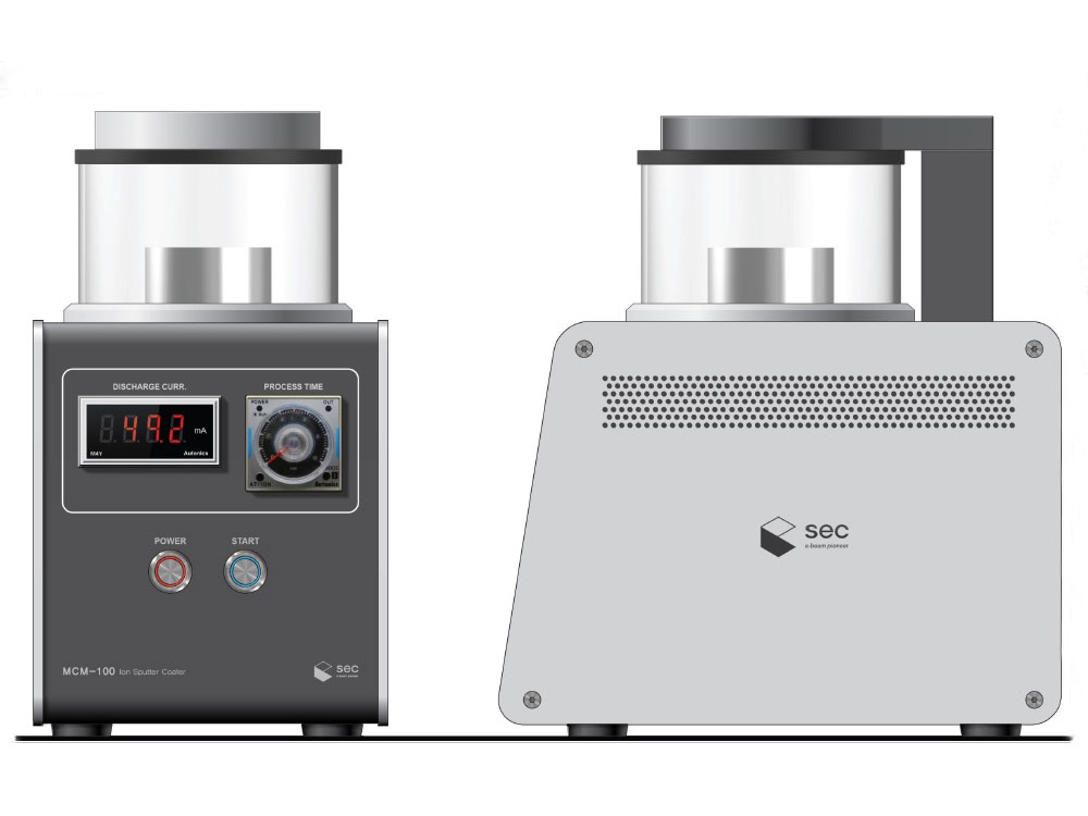
SPUTTER COASTERS

Sample Preparation for Non-Conductive Specimens in Tabletop SEM

cpd

CRITICAL POINT DRIER

STEM Adapter for Basic TEM Imaging Using Standard 3mm Grid Supported Specimens and Particles

Anti-vibration

ANTI-VIBRATION OPTIONS

The BM-8 bench top platform offers 10-100 times better performance than a full size air table in a package only 4.6 inches tall, and without air or electricity!

coming-soon

SEM ACCESSORIES

The SEMs come with a list of standard accessories that are useful for normal operation. When your samples or application are not normal, we are glad to work with you to customize holders and accessories as needed to fit your application.

Industrial Linear Accelerators

Designed for Special Non Destructive Testing (NDT) Applications and for Usage in Scanning Devices for Cargo and Vehicles Inspection at Ports and Borders

img9

LINASEC SERIES

All-In-One System which Includes All Necessary Components, the Linear Accelerator, RF generator, High frequency modulator, HVPS, Shielding, Power Supplies, Interfaces

How do SEMs work?

By scanning a focused beam of electrons, SEMs create magnified detailed images of an object. They create an image through the detection of reflected or knocked-off electrons, unlike in transmission electron microscopes (TEMs), where the electron beam goes straight through the object.

Electrons are emitted using an electron gun, which accelerates the microscope, passing through a series of lenses and apertures to produce a concentrated beam that then interacts with the surface of a sample.

The sample is placed on a stage in the microscope chamber before forming a vacuum in the chamber through a series of pumps. The microscope’s design determines the vacuum level, although some microscopes are built to operate in low vacuum environments, which means the chamber does not need to be evacuated.

Scan coils regulate the position of the electron beam above the objective lens. These coils allow the beam to scan across the sample’s surface, collecting data about a specific area in the process. The interaction between the sample and the electron produces various signals, including secondary electrons, backscattered electrons, and characteristic X-rays, detected by detectors. Finally, these detectors generate the images that are then displayed on a computer screen.

The Role of Electrons in SEMs

Electron microscopes, as the name suggests, use an electron beam for imaging. There are a variety of products formed as a result of the interaction between electrons and matter. All these different types of signals carry various kinds of helpful information about the sample. It’ll be up to you as the microscope operator to decide which signal you want to capture.

An SEM detects two types of electrons in particular:

• Backscattered electrons (BSE)
• Secondary electrons (SE)

After elastic interactions between the beam and the sample, backscattered electrons are reflected. On the other hand, secondary electrons come from the atoms of the sample as a result of inelastic interactions between the electron beam and the sample itself.

BACKSCATTERED ELECTRONS

BSE originates from deeper regions of the sample. These type of electrons come from a broad area inside the interaction volume. They are the product of elastic collisions of electrons with atoms, which cause the electrons’ trajectory to change.

Solid-state detectors that usually contain p-n junctions are the most commonly used BSE detectors. The working principle here is based on the generation of electron-hole pairs by backscattered electrons that escape the sample and are absorbed by the said detectors.

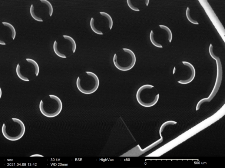
The BSE detectors are symmetrically divided and positioned over the sample, concentrically to the electron beam in a “doughnut” set up to maximize the collection of backscattered electrons. When all parts are enabled, the image’s contrast depicts the element’s atomic number Z. Topographical information from the image, on the other hand, can be retrieved by allowing only specific quadrants of the detector.

SECONDARY ELECTRONS

Meanwhile, SE come from the surface or near-surface regions of the sample. They have lower energy than backscattered electrons but come in handy when you need to perform an inspection of the sample’s surface topography.

The Everhart-Thornley detector is the most commonly used device for SE detection. It consists of a positively charged scintillator inside a Faraday cage that attracts the SE. The scintillator is then used to accelerate the electrons and transform them into light until they reach a photomultiplier for amplification. The SE detector is angled against the side of the electron chamber to maximize the efficiency of detecting secondary electrons.

As a result, BSE and SE contain different types of information. BSE images are susceptible to differences in atomic number: the higher the atomic number, the brighter the material appears in the resulting image. On the other hand, more detailed surface information is obtained through SE imaging.

Since not all SEM users require the same details, the flexibility of having several detectors makes the SEM a very versatile tool that provides practical solutions for a wide range of applications. Among other things, it’ll help you save time, improve the resolution of images, and even automate your analyses.

All About SEMs

ADVANTAGES

The following are the advantages that an SEM offer:

  • Generates highly detailed three-dimensional and topographical images
  • User-friendly software
  • Straightforward to operate with proper training
  • Quick scans are possible (analyses of backscattered electrons (BSE), energy-dispersive X-ray spectroscopy (EDS), and secondary electron imaging (SEI) can be performed within a few minutes)
  • Samples only require a bit of preparation

DISADVANTAGES

Meanwhile, the following are the disadvantages of using an SEM:

  • Costly to purchase and operate
  • Bulky (can take up lots of space)
  • Requires an environment that’s free of electric, magnetic, or vibration interference
  • A qualified operator is required to prepare the samples and operate the microscope
  • Presents a minor risk of radiation exposure
  • Samples must be small enough to fit into the vacuum chamber
  • Cool water and a steady voltage are a requirement

Resolution

The size of the electron spot determines the spatial resolution of an SEM. Unlike traditional image-forming cameras (film or CCD array), an SEM generates an image by rapidly scanning an electron beam over a specimen sample. SEM resolution is typically around 10 nanometres (nm).

Several factors determine the maximum resolution for an SEM image, such as the accelerating voltage, sample type, sample preparation. SEMs can achieve high resolutions that are less than 1 nanometre (nm) but not atomic resolutions. The majority of modern SEMs have a resolution of 1-20 nm, while smaller desktop models have a resolution of 20 nm or higher.

Cost

The cost of procuring SEMs varies. Tabletop models range in price from $60,000 to $120,000 USD, while traditional SEMs (tungsten source) range in price from $120,000 to $250,000 USD. These figures may also vary depending on the country from which you will purchase the SEM.