Desktop SEM Systems
Research-grade imaging in a compact, benchtop form factor. Built by microscopists, for microscopists.
Scanning Electron Microscopes
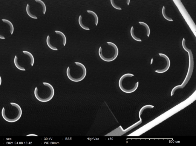
NanoImages sells and leases the SNE-Alpha desktop SEM—a research-grade instrument with 5nm resolution, 250,000x magnification, and 90-second vacuum time in a compact benchtop form factor.
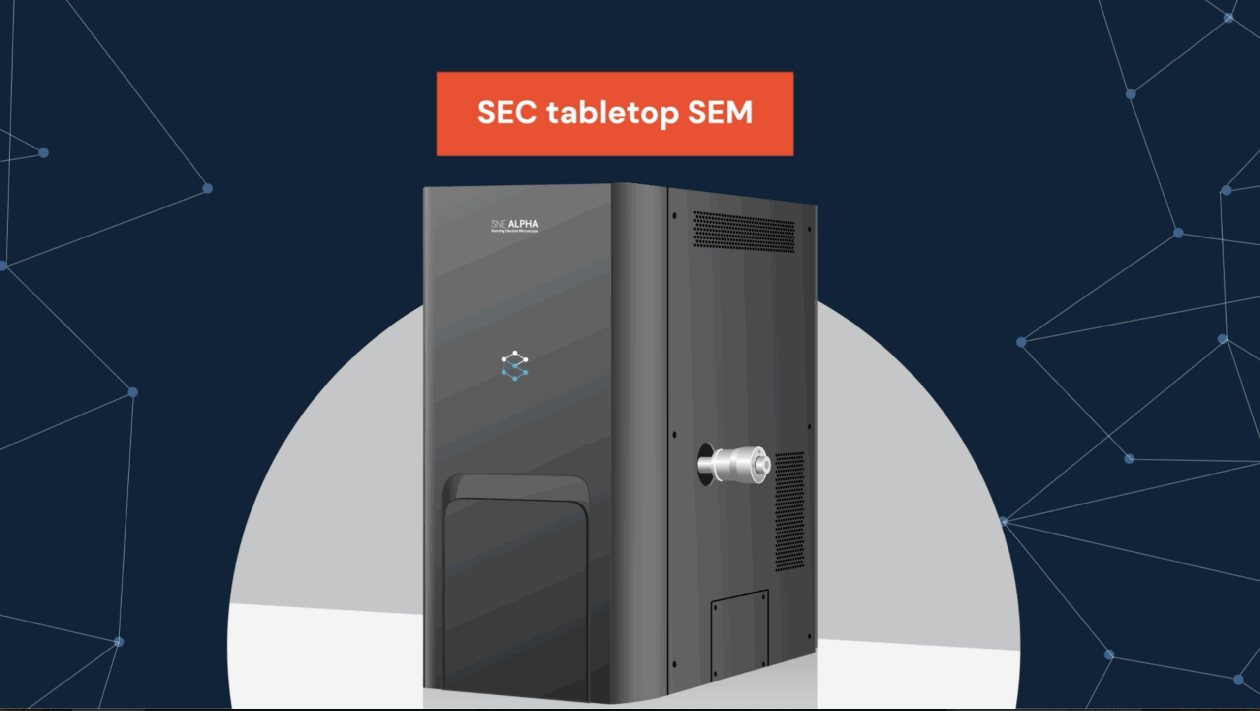
SNE-Alpha
Our flagship desktop SEM delivers floor-model performance with benchtop convenience. Perfect for materials science, life sciences, and quality control.
Microscopist’s note: The SNE-Alpha’s electron optics consistently resolve sub-20nm features in our applications lab. We use it daily for everything from pharmaceutical particle sizing to semiconductor failure analysis—the 90-second vacuum and 15-second vent make high-throughput workflows practical.View Details
Accessories & Add-ons
Expand your SNE-Alpha with EDS elemental analysis, EBSD crystallography, Raman spectroscopy, cathodoluminescence, EBIC, and sample preparation tools.

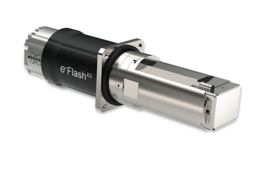
Bruker XFlash 630 EDS
Silicon drift detector for elemental analysis. Detects Boron to Uranium with quantitative accuracy.
Microscopist’s note: We pair this with every SNE-Alpha install—the energy-dispersive X-ray spectroscopy workflow identifies unknown inclusions in under 60 seconds.
EBSD
Electron backscatter diffraction for crystallographic analysis. Map grain orientation and phase identification.
Microscopist’s note: Particularly powerful for metallurgy—we map grain boundaries in welded joints and rolled steel to predict failure modes before they happen.
Cathodoluminescence (CL)
Detect light emission from electron beam excitation. Reveals defects, impurities, and material properties.
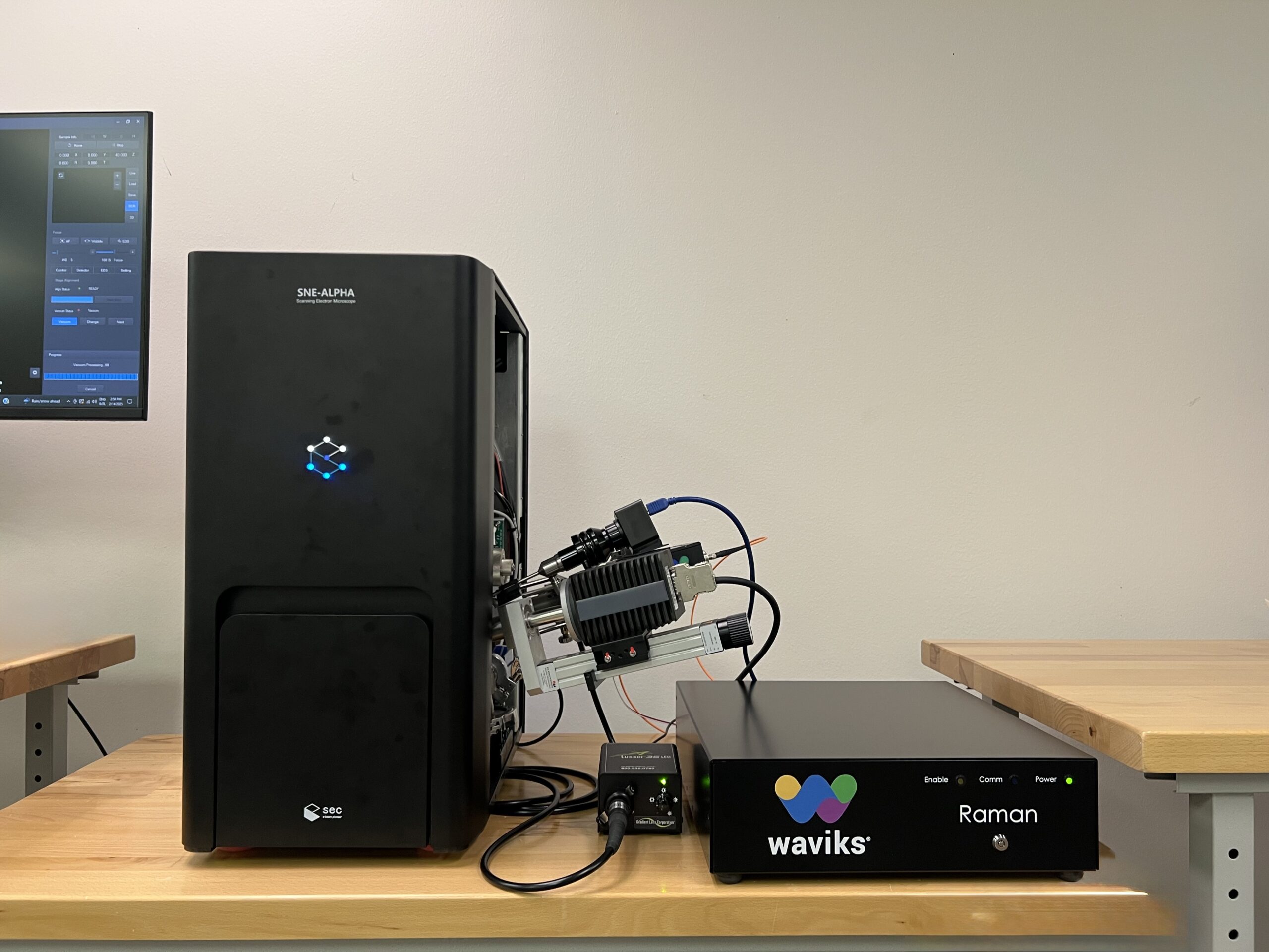
Raman Spectroscopy
Correlative SEM-Raman for molecular identification. Chemical analysis at the nanoscale.
Microscopist’s note: SEM-Raman correlation lets you morphologically image a particle and chemically identify it in the same session—invaluable for pharmaceutical polymorphism screening.
EBIC
Electron beam induced current imaging. Characterize semiconductor junctions and defects.
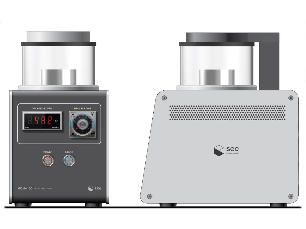
MCM-100 Sputter Coater
Gold, platinum, or carbon coating for non-conductive samples. Compact benchtop design.
Not sure which system is right for you?
Our applications team can help you choose the perfect configuration for your research needs.
Talk to an Expert