The Challenge of Imaging Non-Conductive Samples
Scanning electron microscopy (SEM) delivers high-resolution imagery of microscopic structures, but not all specimens are naturally suited for it. Insulating materials—such as polymers, biological tissues, and ceramics—present a major challenge: they accumulate charge when exposed to the electron beam. This charging disrupts imaging, resulting in distorted visuals that obscure critical details.
Common visual artifacts include:
- Blurred or washed-out regions due to erratic electron scattering
- Bright, overexposed hotspots caused by concentrated surface charge
- Loss of contrast, which makes fine surface structures hard to resolve
Although low-voltage imaging and low-vacuum SEM modes are sometimes employed to reduce charging, these methods typically compromise image quality. Reduced resolution and increased noise remain significant limitations.
Why Conductive Coatings Are Essential
Sputter coating provides an elegant, effective solution. By depositing a nanometer-thin conductive metal layer over the sample, excess electrons gain a path to dissipate. This eliminates surface charging and stabilizes the imaging environment.
Key benefits include:
- Charge mitigation: The conductive layer forms a continuous path for electron drainage
- Signal clarity: By reducing noise from charge accumulation, signal-to-noise ratios improve significantly
- Structural integrity: With no electrostatic distortion, fine morphological details are preserved
- Higher magnification: With charging suppressed, SEM can operate at ultra-high magnifications without focus drift or blurring
In short, sputter coating transforms problematic specimens into stable, image-ready targets.
Sputter Coating vs. Low-Vacuum SEM Modes
Low-vacuum SEM introduces a gas (often water vapor or nitrogen) into the chamber to neutralize surface charge on uncoated samples. While this helps reduce charging, it introduces its own limitations:
- Reduced resolution: Gas molecules scatter electrons, softening the beam and lowering image sharpness
- Lower contrast: Detector efficiency drops in low-vacuum conditions
- Limited detail: Ultra-fine features are often lost or obscured
For applications that demand high-resolution and nanoscale visibility, sputter coating remains the preferred approach. It enables true high-vacuum imaging, where the full performance of modern SEM instruments can be realized.
Choosing the Right Coating for Your Sample
Material selection and coating thickness are critical to effective sputter coating.
Common Coating Materials
- Gold (Au): Offers excellent conductivity and a fine grain size, making it ideal for high-resolution imaging
- Platinum (Pt) or Iridium (Ir): Preferred for ultra-fine detail due to their smaller grain sizes
- Carbon (C): Used when Energy Dispersive Spectroscopy (EDS) is required, as carbon does not interfere with most X-ray signals
Optimal Thickness
A coating thickness of 5–15 nm typically suffices. Thicker coatings can obscure surface features, so minimal effective coverage is best.
Best Practices
- Use a high-vacuum coater for uniform, fine-grained films
- Avoid pre-coating beam exposure on sensitive samples
- Handle coated specimens carefully to avoid damaging the delicate surface film
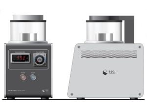
Introducing the MCM-100 Ion Sputter Coater by NanoImages
For labs seeking a streamlined solution for high-resolution SEM imaging, the MCM-100 Ion Sputter Coater delivers precision, efficiency, and ease-of-use:
Key Features
- Integrated vacuum system: Compact design with built-in pump and plasma chamber
- Automated cycles: Programmable parameters and one-button operation ensure consistency
- Rapid processing: Coating cycles completed in minutes
- Controlled nanolayers: Deposits uniform Au or Pt films just a few nanometers thick
- Versatile compatibility: Suitable for diverse materials—from biopolymers to geological specimens
Performance Impact
With the MCM-100, even benchtop SEMs achieve clarity previously reserved for high-end systems. Labs consistently report sharper images, cleaner contrast, and greater reproducibility across diverse non-conductive materials.
FAQs
Why not just use low-voltage SEM to avoid charging?
Low-voltage modes reduce beam energy but also limit resolution and contrast. Sputter coating allows full-voltage, high-magnification operation without these compromises.
Will sputter coating affect EDS results?
It can. If you plan to perform EDS, consider using carbon coating or ensure the coating material doesn't interfere with your elemental peaks.
Can all non-conductive samples be sputter coated?
Most can, including biological, polymeric, and ceramic materials. For sensitive samples, low-energy sputtering techniques are recommended.
Final Thoughts
Sputter coating is not just a preparatory step—it's an enabler for unlocking the full resolution potential of SEM. By addressing the root cause of image degradation in insulating samples, it ensures clarity, contrast, and reproducibility at the nanoscale.
For researchers, engineers, and analysts working with challenging specimens, integrating sputter coating into the SEM workflow is an investment in image quality and data integrity. And with tools like the MCM-100, achieving professional-grade results has never been more accessible.
Ready to transform your SEM imaging? Explore the NanoImages MCM-100 and experience the clarity that conductive nano-coatings deliver.