Posts by AZO
Why Choose EBIC Techniques for Solar Panel Inspection?
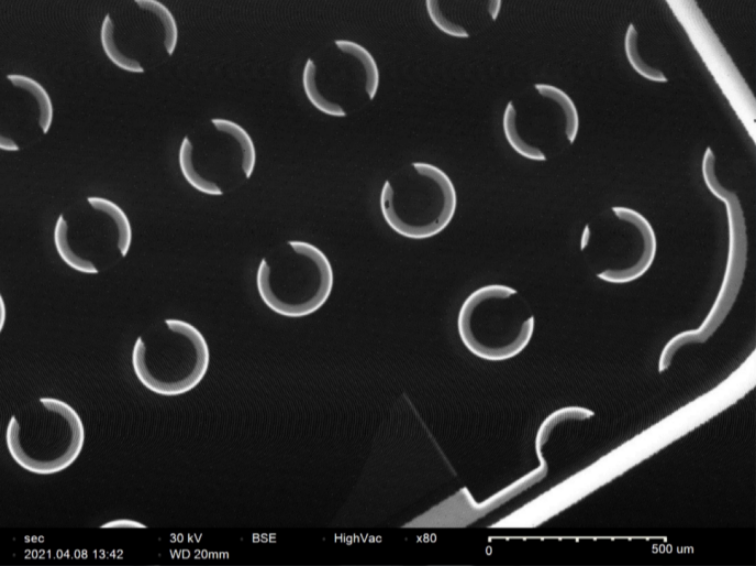
Ensuring Solar Cell Quality Solar panels are made up of many interconnected photovoltaic cells, and even microscopic defects within a single cell can diminish overall efficiency and lifespan. While methods like optical inspection, infrared thermography, and electroluminescence (EL) imaging provide valuable macroscopic views, they lack the spatial resolution to detect subtle internal faults. Electron beam…
Read MoreKey Benefits of SEM for Mineral Phase Analysis
Why Use SEM-EDS for Mineral Identification Determining mineral phases within a sample is essential for geologists, mining engineers, and materials scientists. Traditional techniques like X-ray diffraction (XRD) yield bulk compositional data but lack spatial resolution. Optical microscopy, while providing structural context, is resolution-limited and relies heavily on subjective interpretation. Scanning electron microscopy (SEM), especially when…
Read MoreHow Sputter Coating Unlocks High-Resolution SEM
The Challenge of Imaging Non-Conductive Samples Scanning electron microscopy (SEM) delivers high-resolution imagery of microscopic structures, but not all specimens are naturally suited for it. Insulating materials—such as polymers, biological tissues, and ceramics—present a major challenge: they accumulate charge when exposed to the electron beam. This charging disrupts imaging, resulting in distorted visuals that obscure…
Read MoreCombining Forensic SEM and Raman for Gunshot Residue Detection
Gunshot Residue Evidence: A Two-Part Puzzle When a firearm is discharged, it releases a complex cloud of microscopic debris known as gunshot residue (GSR). This residue comprises both inorganic particles from the primer and organic compounds from the propellant. Traditional GSR detection relies heavily on scanning electron microscopy coupled with energy dispersive X-ray spectroscopy (SEM/EDS),…
Read MoreUsing Raman-SEM for Correlative Imaging in Biology
Merging Structure and Chemistry When it comes to studying biological systems, visualizing structure and understanding chemistry often require different tools. Scanning electron microscopy (SEM) excels at showing ultrastructural details—down to the nanometer scale—of cells, tissues, and biomaterials. Raman spectroscopy, on the other hand, provides a label-free molecular fingerprint of those structures. By integrating these two…
Read MoreKey Benefits of Using EBSD for SEM Aerospace Applications
Microstructure Matters in Aerospace Turbine blades shear through superheated air at thousands of revolutions per minute. Engine disks withstand crushing loads with millisecond precision. These aerospace components owe their resilience to engineered microstructures. Electron backscatter diffraction (EBSD), paired with scanning electron microscopy (SEM), maps grain orientations and boundary types with precision. Engineers use this data…
Read MoreHow Does EBDS Analysis Work?

Electron Backscatter Diffraction (EBSD) is a powerful technique used in conjunction with Scanning Electron Microscopy (SEM) to analyze the crystallographic structure of materials. This integration allows researchers to study grain structures, phase distributions, and strain patterns at the microscale, offering valuable insights for materials science, metallurgy, and geoscience applications. By combining EBSD with SEM, researchers…
Read MoreUnderstanding SEM Integration with Electron Beam Induced Current (EBIC)
Electron Beam Induced Current (EBIC) is a powerful analytical technique used to study electronic properties of materials, particularly semiconductors and photovoltaic devices. When integrated with Scanning Electron Microscopy (SEM), EBIC provides detailed insights into charge carrier behavior, defect structures, and junction performance. This combination enables researchers to correlate electrical activity with microstructural features, making it…
Read MoreUsing Cathodoluminescence in SEM Analysis

Cathodoluminescence (CL) spectroscopy is a powerful technique used to study the optical and electronic properties of materials by analyzing light emitted when a material is exposed to an electron beam. When integrated with Scanning Electron Microscopy (SEM), CL provides unique insights into a sample’s composition, crystallinity, and defect structures at the microscale. This hybrid approach…
Read MoreHow to Integrate Raman Spectroscopy with Scanning Electron Microscopy (SEM)
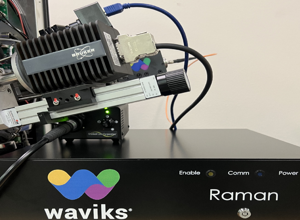
Raman spectroscopy and Scanning Electron Microscopy (SEM) are two powerful analytical techniques that, when combined, provide an unprecedented level of material characterization. The integration of these methods allows researchers to simultaneously acquire high-resolution structural images and detailed molecular or chemical information, making it particularly valuable in materials science, nanotechnology, and semiconductor research. Fundamental Principles of…
Read More