
Semiconductors
Wafer inspection, defect analysis, process development, and quality control
The SNE-Alpha desktop SEM is used in semiconductor fabs and R&D labs for device inspection, cross-section analysis, solder joint review, and ESD failure analysis. At 5nm resolution and 30kV, it resolves sub-10nm features. Pair with the Bruker XFlash EDS for elemental mapping of die layers and interconnects. See full SNE-Alpha specifications →
The microelectronic devices we enjoy and depend on today would not be possible without electron microscopy. From R&D to production QC, scanning electron microscopy provides the resolution and analytical capabilities essential for semiconductor manufacturing and failure analysis.
The SNE-Alpha desktop SEM delivers the imaging performance needed for semiconductor applications in a compact, accessible format. With 5nm resolution, 1-30kV accelerating voltage range, and optional EDS integration, you can characterize devices with both high-resolution morphological imaging and elemental analysis.
Key Semiconductor Applications
- Wafer Inspection: Examine surface defects, contamination, and process variations across wafer surfaces
- Defect Analysis: Identify and characterize crystallographic defects, particles, and foreign materials
- Cross-Section Analysis: Measure layer thicknesses, via profiles, and interface quality
- Failure Analysis: Investigate device failures, electrical shorts, and manufacturing defects
- Process Development: Optimize etch profiles, deposition uniformity, and lithography patterns
- Particle Identification: Combine SEM imaging with EDS to identify contamination sources
Why Desktop SEM for Semiconductors?
While many semiconductor fabs rely on large floor-model SEMs, a desktop SEM like the SNE-Alpha offers significant advantages for certain applications:
- Fast Turnaround: 90-second pump-down means quick sample inspection without waiting for central lab availability
- Point-of-Use: Locate the SEM near your cleanroom or process line for immediate feedback
- R&D Flexibility: Ideal for university research, startups, and development labs
- Cost Effective: Lower capital and operating costs than floor-model alternatives
Semiconductor SEM Images
Sample images captured with the SNE-Alpha desktop SEM. Click to enlarge.
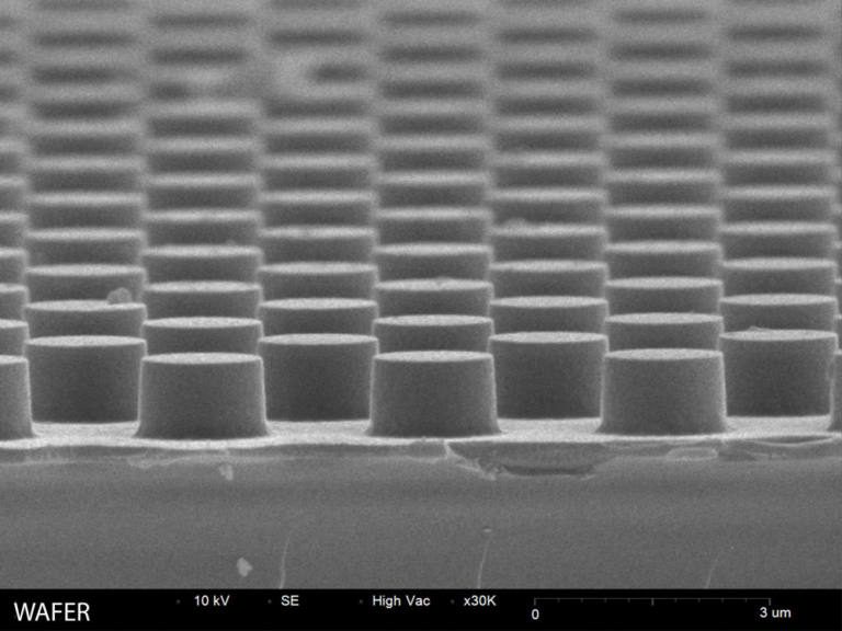
Silicon Wafer
Wafer surface inspection showing pattern and features
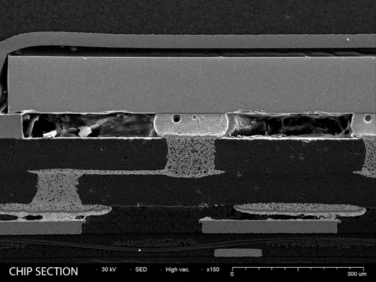
Chip Cross-Section
Integrated circuit cross-section showing layer structure
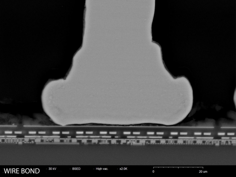
Wire Bonding
Gold wire bond connection to chip bond pad
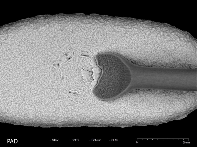
Bond Pad
Wire bond pad surface texture and interface
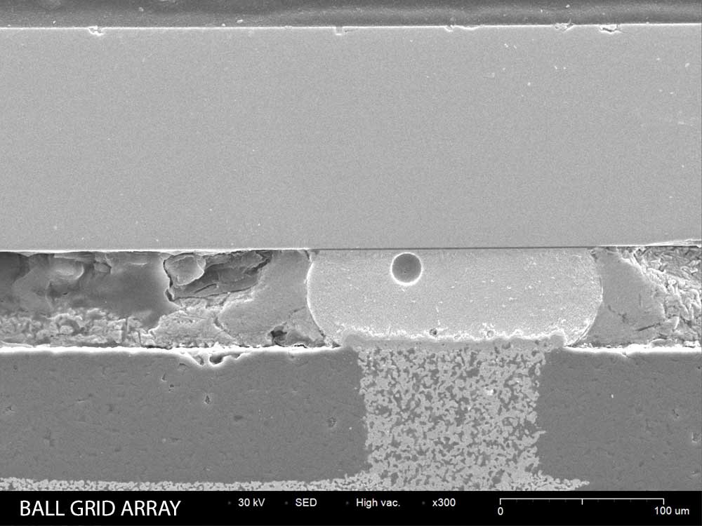
BGA Package
Ball grid array solder joint inspection
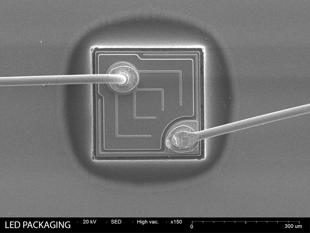
LED Packaging
LED die and wire bond assembly inspection
Recommended Analytical Techniques
SE Imaging
High-resolution topographic imaging for surface features, patterns, and structures.
BSE Imaging
Compositional contrast to distinguish materials and detect buried features.
EDS Analysis
Elemental identification of particles, contamination, and layer composition.
EBIC
Electron beam induced current for junction visualization and defect localization.
Recommended Equipment
SNE-Alpha Desktop SEM
Compact, high-resolution scanning electron microscope ideal for research and quality control applications.
Bruker XFlash EDS
Energy dispersive X-ray spectroscopy for elemental analysis and material identification.
MCM-100 Sputter Coater
Prepare non-conductive samples with gold or platinum coatings for optimal SEM imaging.
Related Applications
Resources
Explore Semiconductor Applications
See how the SNE-Alpha can support your semiconductor research and QC needs.