
Materials Science
Comprehensive materials characterization for metals, polymers, composites, ceramics, and failure analysis
The SNE-Alpha desktop SEM is the leading compact instrument for materials science applications — failure analysis, microstructure characterization, fracture surface imaging, and grain structure studies. With 5nm resolution at 30kV and a 90-second pump-down, it fits on a bench, needs no specialist operator, and handles metals, polymers, ceramics, and composites. See full SNE-Alpha specifications →
Materials science spans the study of all material classes—metals, polymers, ceramics, composites, and advanced materials. Scanning electron microscopy is the cornerstone analytical technique for understanding structure-property relationships, from microstructure to nanoscale features.
The SNE-Alpha desktop SEM delivers the resolution and analytical capabilities that materials scientists need without the footprint or complexity of floor-model systems. As the leading Tabletop SEM distributor in the US, NanoImages provides expert support for every materials science application. With 5nm resolution and integrated EDS capability, you can image surface morphology, analyze microstructure, and determine elemental composition all in one instrument.
Key Materials Science Applications
- Failure Analysis: Investigate fracture surfaces, corrosion, fatigue cracks, and manufacturing defects. BSE imaging reveals compositional variations while EDS identifies contaminants
- Microstructure Analysis: Characterize grain size, phase distribution, and crystallographic features. Essential for understanding mechanical properties and processing effects
- Coating and Surface Analysis: Measure coating thickness, evaluate adhesion, and inspect surface treatments. Cross-sectional imaging reveals layer structure
- Polymer Characterization: Examine polymer morphology, blend compatibility, filler distribution, and degradation mechanisms
- Composite Materials: Analyze fiber-matrix interfaces, void content, and damage mechanisms critical for aerospace and automotive applications
- Quality Control: Routine inspection of incoming materials, in-process components, and finished products for specification compliance
Material Classes
The SNE-Alpha handles the full range of materials:
- Metals and Alloys: Steels, aluminum, titanium, superalloys, and precious metals
- Polymers: Thermoplastics, thermosets, elastomers, and polymer blends
- Ceramics: Oxides, carbides, nitrides, and glass materials
- Composites: Carbon fiber, glass fiber, metal matrix, and ceramic matrix composites
- Coatings: Thermal barrier coatings, hard coatings, corrosion protection, and thin films
Materials Science SEM Images
Sample images captured with the SNE-Alpha desktop SEM.
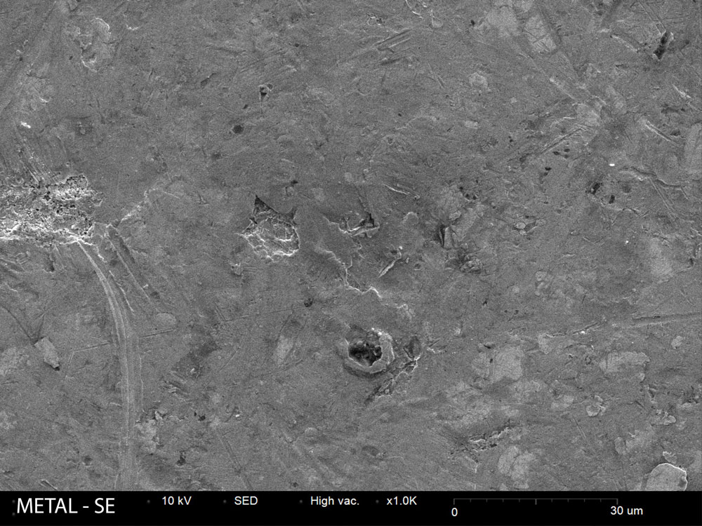
Metal Microstructure
Secondary electron imaging showing surface topography
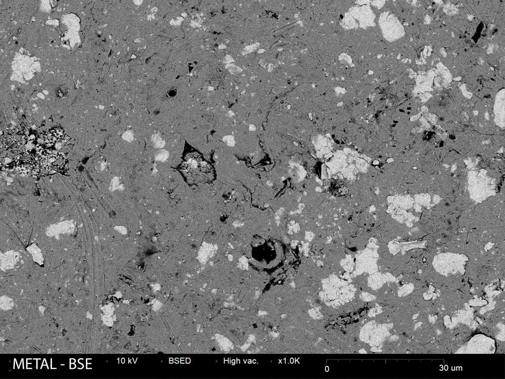
Compositional Contrast
Backscattered electron imaging revealing phase contrast
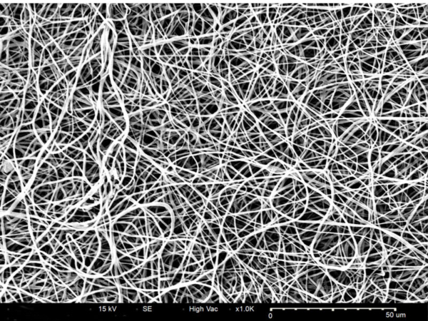
Fiber Composite
Fiber cross-section analysis for composite materials
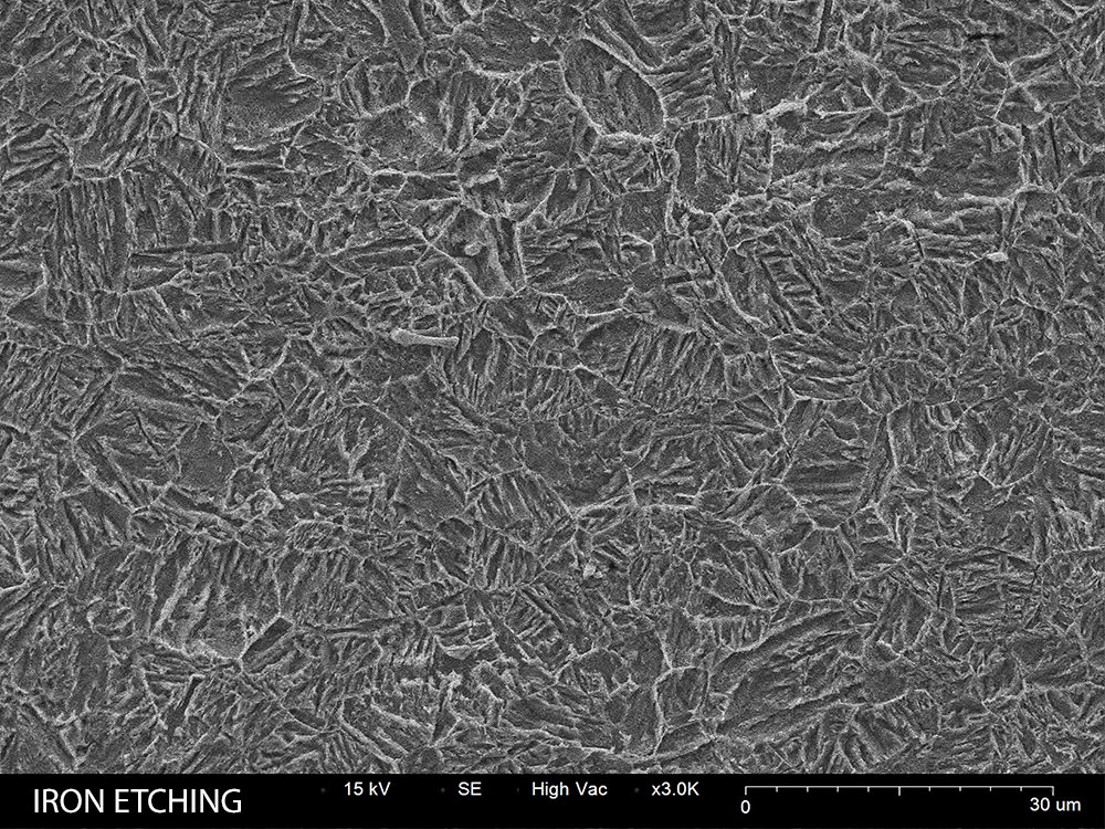
Etched Metal
Chemically etched surface showing grain structure
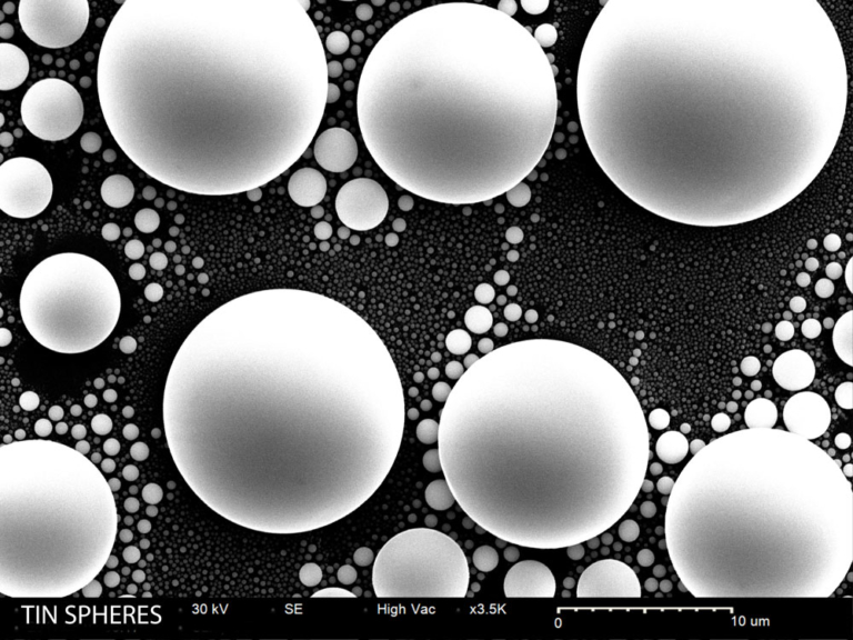
Metal Powder
Spherical powder for additive manufacturing
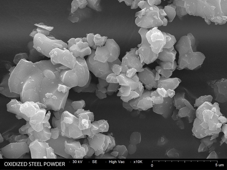
Steel Powder
Powder particle morphology and surface oxidation
Why Materials Scientists Choose the SNE-Alpha
5nm Resolution
Resolve fine microstructural features, nanoscale defects, and thin film structures with clarity.
Dual Detectors
SE for topography, BSE for composition. Switch instantly between imaging modes.
90-Second Vacuum
High sample throughput for production environments and QC laboratories.
EDS Integration
Add Bruker XFlash EDS for elemental analysis, phase identification, and composition mapping.
Large Chamber
Accommodate bulk samples up to 70mm diameter without extensive sectioning.
Simple Operation
Get results fast—intuitive software means no dedicated operator required.
Recommended Equipment
SNE-Alpha Desktop SEM
Compact, high-resolution scanning electron microscope ideal for research and quality control applications.
Bruker XFlash EDS
Energy dispersive X-ray spectroscopy for elemental analysis and material identification.
MCM-100 Sputter Coater
Prepare non-conductive samples with gold or platinum coatings for optimal SEM imaging.
Related Applications
Resources
Ready to See Your Materials in Detail?
Send us your samples and we’ll show you exactly what the SNE-Alpha can reveal.