The SNE-Alpha desktop SEM is used across 17+ research disciplines — from materials science and forensics to pharmaceutical QC and semiconductor failure analysis. With 200+ peer-reviewed publications, it is the most documented tabletop SEM in US research. All applications benefit from the same core advantage: research-grade SEM imaging in 90 seconds, on a standard lab bench, without a dedicated room.
Desktop SEM Applications Across 17 Industries
From nanoparticles to biological tissues, the SNE-Alpha delivers publication-ready images across every field of research.
Explore Our Applications

Materials Science
Characterize metals, polymers, composites, and ceramics at the nanoscale. Analyze grain structure, fracture surfaces, coating thickness, and phase distribution for research and quality control.
Explore materials science SEM applications
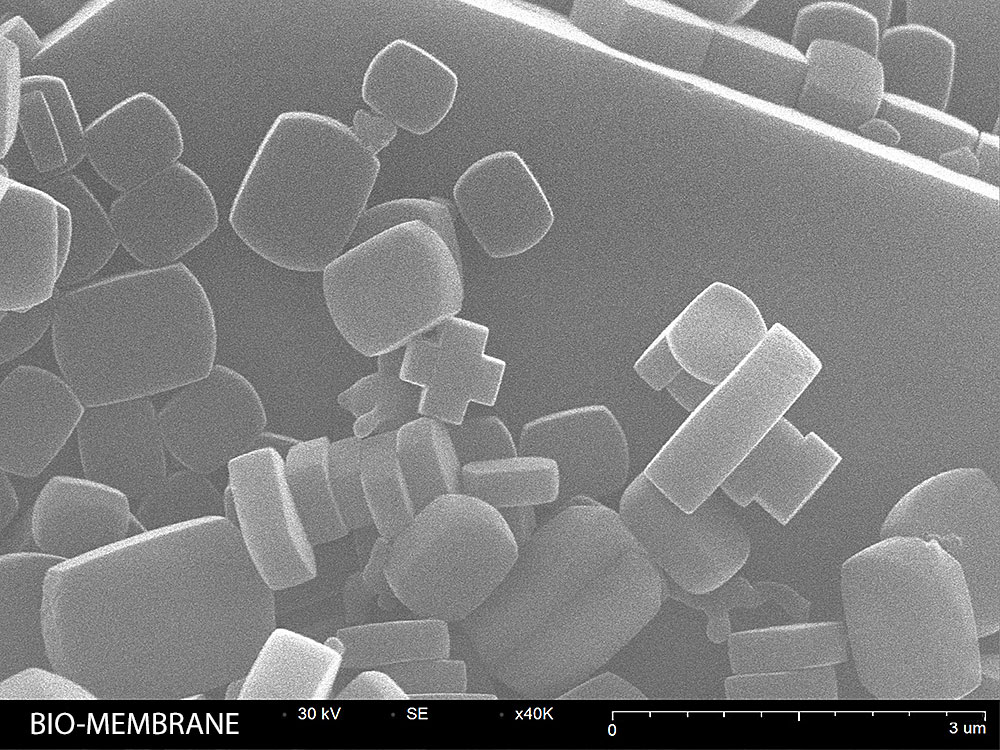
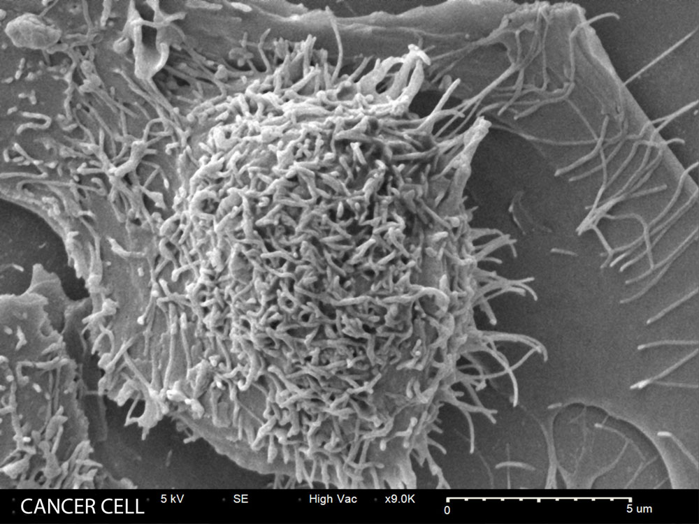
Life Sciences
Image cells, tissues, bacteria, and biological structures with nanometer resolution. Ideal for morphology studies, surface characterization, and cellular ultrastructure research.
Explore life science SEM applications
Forensics
Analyze gunshot residue (GSR), fibers, paint chips, and trace evidence with SEM-EDS. Elemental identification meets ASTM E1588 standards for forensic laboratories.
Explore forensic SEM applications
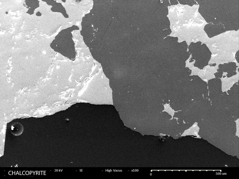
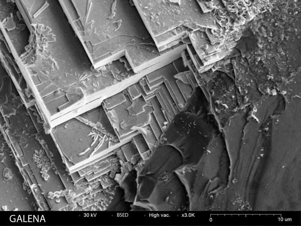
Geology & Mining
Study minerals, rock formations, fossils, and ore samples. Determine composition with EDS for mineral identification, petrographic analysis, and resource exploration.
Explore geology SEM applications
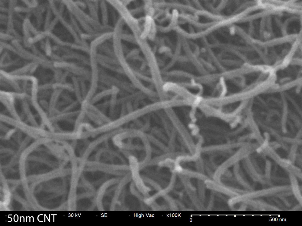
Nanomaterials
Characterize nanoparticles, quantum dots, carbon nanotubes, and thin films. The SNE-Alpha’s 5nm resolution reveals nanoscale morphology and size distribution.
Explore nanomaterials SEM applications
Pharmaceuticals
Analyze drug particles, excipients, and formulations for size distribution, surface morphology, and crystalline structure. Essential for QC, R&D, and regulatory compliance.
Explore pharmaceutical SEM applications
Semiconductors
Inspect circuit patterns, wafer defects, and cross-sections with nanometer precision. Quality control and failure analysis for electronics manufacturing and IC packaging.
Explore semiconductor SEM applications
Electronics
Investigate fractures, corrosion, wear, and manufacturing defects in electronic components. Root cause analysis with combined SEM imaging and EDS elemental mapping.
Explore electronics SEM applications
Environmental
Analyze particulates, pollutants, microplastics, and soil samples at high magnification. Critical for environmental monitoring, contamination studies, and regulatory research.
Explore environmental SEM applications
Energy
Study battery electrode materials, solar cell structures, fuel cells, and catalysts. Optimize energy storage and conversion performance through detailed microstructure analysis.
Explore energy SEM applications
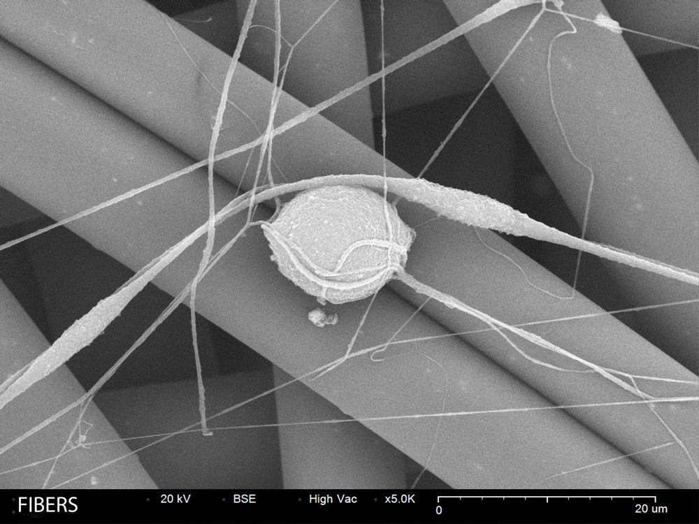
Fibers & Textiles
Examine fiber cross-sections, fabric weave patterns, and surface treatments at the micro level. Quality control and failure analysis for textile manufacturing and forensic fiber comparison.
Explore textile SEM applications
Healthcare
Analyze medical devices, implants, and biomaterials at sub-micron resolution. Quality assurance for healthcare product development, surface biocompatibility, and regulatory testing.
Explore healthcare SEM applications
Chemistry
Investigate crystal structures, precipitates, and catalyst surfaces. Correlate surface morphology with chemical properties using combined SEM imaging and EDS analysis.
Explore chemistry SEM applications
Transportation
Analyze wear patterns, protective coatings, and failure modes in automotive and rail components. Quality control and root cause analysis for transportation material certification.
Explore transportation SEM applications
Aerospace
Inspect turbine blades, composites, and thermal barrier coatings. Critical microstructure analysis for aerospace material certification, fatigue testing, and failure investigation.
Explore aerospace SEM applicationsMetallurgy
Analyze alloy microstructures, grain boundaries, and phase distributions. Study heat-treatment effects, inclusion characterization, and weld integrity for metals research and QC.
Explore metallurgy SEM applications
Other Cool Stuff
From 3D printing and art conservation to food science and cosmetics — discover unexpected desktop SEM applications that push the boundaries of electron microscopy imaging.
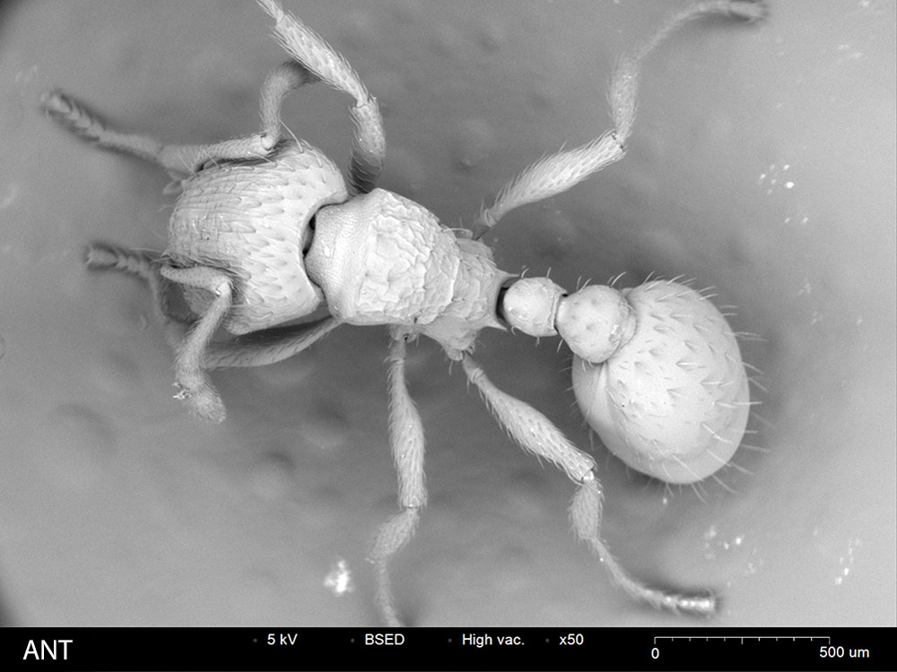
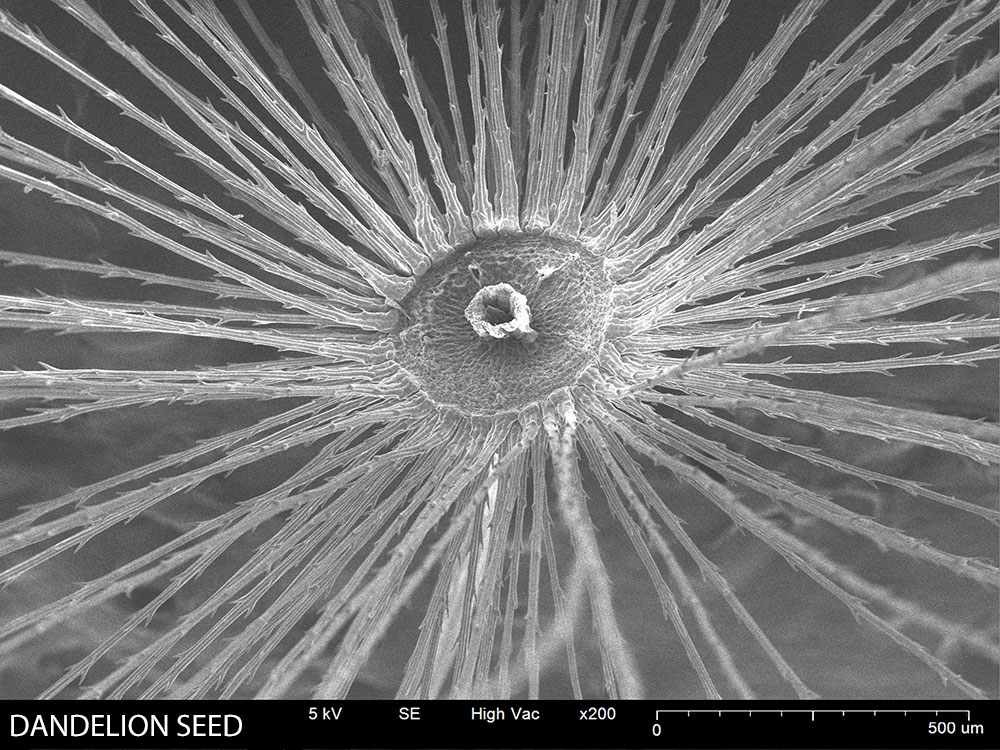
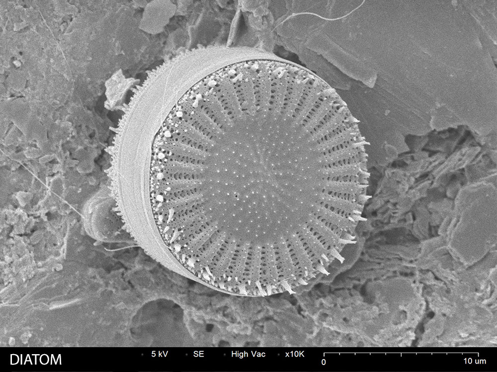
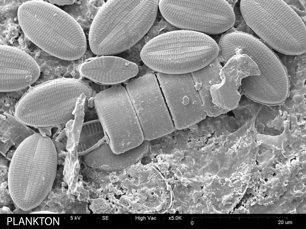
Explore unique SEM applicationsSample Images
Every image below was captured on an SNE-Alpha desktop SEM. Click any image to view full resolution with acquisition parameters.
Have a Specific Application?
Our applications team can help you determine if the SNE-Alpha is right for your research needs.
Request a Quote