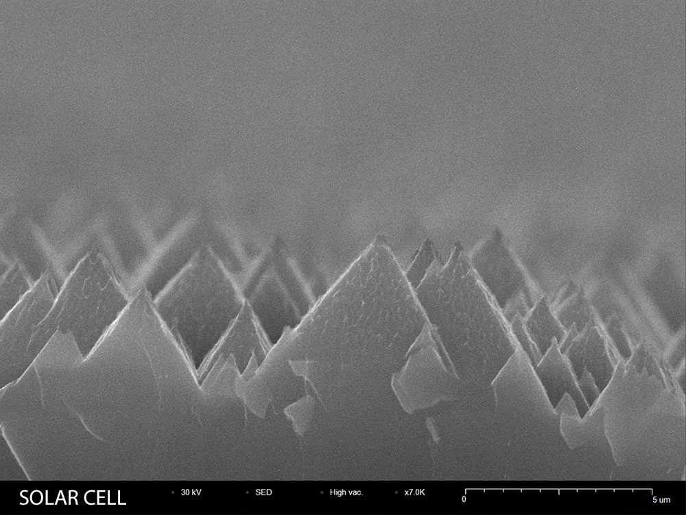
Ensuring Solar Cell Quality
Solar panels are made up of many interconnected photovoltaic cells, and even microscopic defects within a single cell can diminish overall efficiency and lifespan. While methods like optical inspection, infrared thermography, and electroluminescence (EL) imaging provide valuable macroscopic views, they lack the spatial resolution to detect subtle internal faults. Electron beam induced current (EBIC) imaging, performed within a scanning electron microscope (SEM), offers a way to map the electrical behavior of solar cells at the micro-scale.
By scanning a focused electron beam and recording the induced current from a biased solar cell, EBIC reveals local variations in electrical activity. It shows which areas are actively contributing to current generation and which are not—making it a powerful diagnostic tool for both manufacturing quality control and photovoltaic research.
How EBIC Works for Solar Cells
Microscale Current Mapping
EBIC imaging involves rastering an electron beam across a solar cell under electrical bias. As the beam interacts with the semiconductor, it generates electron-hole pairs. In well-functioning regions, these pairs are efficiently separated and collected, generating measurable current. At defect sites, recombination dominates, and the induced current drops.
The result is a contrast image: bright regions indicate strong current generation; dark regions point to defects or electrically inactive zones. This micro-current map overlays directly onto SEM imagery, enabling defect localization down to sub-micron scales.
Revealing Hidden Defects
EBIC excels at pinpointing flaws that standard techniques often miss:
- Grain Boundaries & Microcracks: In multicrystalline silicon cells, grain boundaries appear as dark lines due to increased recombination. EBIC can also detect microcracks, shunts, or laser-induced damage from fabrication steps.
- Thin Film and Next-Gen Materials: In technologies like CdTe, CIGS, or perovskites, EBIC reveals non-uniformities, grain-to-grain variation, or phase-related issues invisible to optical tests.
This depth of insight supports both process refinement and failure diagnostics across a range of photovoltaic technologies.
Key Benefits of EBIC in PV Inspection
Early Detection of Microscopic Issues
EBIC allows early-stage detection of microscopic performance bottlenecks. If a manufacturing step introduces minor damage (e.g. laser scribing micro-cracks), EBIC immediately visualizes the problem, enabling corrective action before mass production.
Quantitative Failure Analysis
Beyond visual localization, EBIC provides a semi-quantitative sense of how much current loss is associated with each defect. The contrast between healthy and defective regions indicates the severity of recombination or shunting. Engineers can prioritize which defect types or regions most urgently require mitigation.
Complementary to Other Tests
EBIC doesn’t replace EL or IV testing—it complements them. Where EL shows a general area of underperformance, EBIC clarifies the exact microstructural root cause. Together, they form a layered diagnostic approach, linking macro anomalies to their micro origins.
Implementing EBIC on a Tabletop SEM
Accessible EBIC Solutions
What once required high-end SEMs and complex setups is now achievable on compact platforms. NanoImages offers an EBIC add-on kit for its desktop SEMs. The kit includes a transimpedance amplifier and sample stage connections, transforming any compatible SEM into an EBIC inspection tool.
Users can switch from standard imaging to EBIC mode in seconds. The same platform handles SEM imaging, elemental EDS, and EBIC current mapping, streamlining workflows for quality control labs or R&D facilities.
Non-Destructive and Practical
EBIC is minimally invasive. Plan-view inspection is often possible on intact cells, requiring only electrical contact. Cross-sectional imaging is also feasible for junction-level insights, but sample prep remains straightforward. Because EBIC doesn’t damage the cell, the same sample can undergo multiple analyses or be archived.
Interested in EBIC Techniques for Solar Panel Inspection?
EBIC provides a unique electrical perspective on solar cell behavior. It bridges the gap between microstructure and function, revealing how internal features affect current generation. As photovoltaic technologies evolve, the ability to visualize and quantify electrical activity at the microscopic scale becomes ever more important.
With EBIC, researchers and manufacturers gain a powerful inspection tool that elevates cell performance assessment. And with modern tabletop SEM systems, this capability is more accessible than ever. From detecting fine-scale defects to optimizing materials and processes, EBIC helps ensure that every solar cell delivers maximum efficiency and reliability in the field.