Microstructure Matters in Aerospace
Turbine blades shear through superheated air at thousands of revolutions per minute. Engine disks withstand crushing loads with millisecond precision. These aerospace components owe their resilience to engineered microstructures. Electron backscatter diffraction (EBSD), paired with scanning electron microscopy (SEM), maps grain orientations and boundary types with precision. Engineers use this data to forecast material behavior, fine-tune designs, and guarantee performance under pressure.
EBSD Insights for Aerospace Alloys
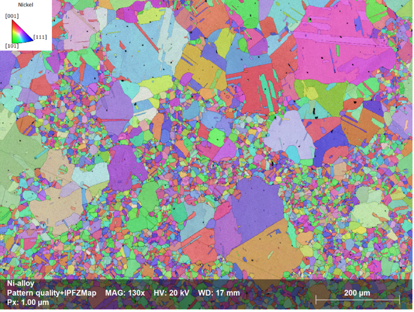
Grain orientation mapping is one of EBSD's hallmark capabilities. It creates visualizations that reveal how grains are aligned within a metal. This information is vital because the texture of an alloy—that is, its preferred grain orientation resulting from manufacturing processes like rolling or forging—directly impacts mechanical properties such as fatigue strength and creep resistance. For example, when abnormal or excessively large grains are identified, it often signals potential failure points. With this knowledge, engineers can adjust processing steps like annealing to create more desirable grain structures.
Phase identification is equally crucial in aerospace applications. Alloys used in flight-critical components, especially nickel superalloys and advanced aluminum grades, often consist of multiple phases with different properties. EBSD, particularly when used alongside Energy Dispersive Spectroscopy (EDS), distinguishes between these phases. It can confirm whether strengthening precipitates such as gamma prime are distributed correctly, or if unwanted brittle phases have formed during heat treatment or service—a common cause of material degradation.
Another advantage of EBSD lies in its ability to analyze grain boundaries. These microstructural features greatly influence corrosion behavior, creep resistance, and fracture propagation. By measuring misorientation angles, EBSD categorizes boundaries into low- and high-angle types. It can also detect networks of weak boundaries that may serve as preferential paths for crack growth. Engineers use this information to improve alloy design or modify processing parameters.

Aerospace Applications of EBSD
In turbine engine components, particularly those made from nickel-based superalloys, EBSD plays a pivotal role. Kernel Average Misorientation (KAM) maps generated from EBSD data highlight areas of localized plastic strain and creep damage. This is especially useful in analyzing regions near cooling holes or stress concentrators. Additionally, the technique verifies whether heat treatments have successfully produced the desired microstructure—whether it's a uniform fine-grained matrix or a directionally solidified structure optimized for high-temperature performance. EBSD also evaluates the condition of thermal barrier coatings, identifying phase changes that occur after service exposure.
When it comes to airframe structures made from aluminum and titanium, EBSD supports both development and failure analysis. By checking grain size and orientation post-forging or rolling, it ensures that grain flow supports mechanical strength and damage resistance. In cases of fracture, mapping the crack path in relation to the grain structure can reveal whether a failure was due to metallurgical anomalies, such as unfavorable textures or inclusions.
Modern joining and fabrication methods like welding and additive manufacturing (AM) also benefit from EBSD. In welds, it maps how thermal cycles affect grain growth in the heat-affected zone and helps validate the welding process by revealing microstructural transitions. In AM components, which are built layer by layer, EBSD provides insight into grain growth direction, anisotropy, and defects such as lack of fusion. This layer-specific analysis often uncovers issues invisible to optical methods, making EBSD indispensable for certifying new manufacturing methods.
Enhancing Aerospace Materials with EBSD
For materials engineers, EBSD data is more than a diagnostic tool—it's a feedback loop that informs alloy development. For instance, when designing new high-temperature alloys, EBSD confirms whether the processing route has produced the intended microstructure. It directly correlates grain size, orientation distributions, and precipitate presence with key performance metrics like creep resistance and fatigue life.
Manufacturing processes can also be fine-tuned based on EBSD findings. If post-process analysis reveals an unfavorable texture or unexpected grain boundary distribution, adjustments to forging temperature, cooling rate, or heat treatment duration can be made to optimize the final structure.
On the production floor, EBSD becomes a powerful tool for quality assurance. Aerospace specifications often require microstructural validation, and EBSD provides a quantitative, reproducible method to meet those demands. Routine EBSD scans detect issues like abnormal grain growth or missing phases before parts are integrated into assemblies. Similarly, EBSD comparisons between in-service and as-manufactured components can reveal gradual microstructural changes, such as phase depletion or grain coarsening. These insights help schedule maintenance and assess service life accurately.
When failures occur, EBSD offers forensic clarity. By mapping the microstructure at fracture sites, it helps determine whether cracks initiated along grain boundaries, at phase interfaces, or due to other microstructural inconsistencies. These findings guide corrective actions in materials design and processing, ultimately enhancing safety and reliability.

EBSD on the Tabletop SEM: Accessible Precision
Until recently, EBSD was limited to high-end SEM platforms operated by experts. Today, NanoImages offers a practical alternative: a compact SEM equipped with the Bruker QUANTAX ED-XS EBSD/EDS system. This integration brings powerful crystallographic and chemical analysis directly to the lab bench.
The benefits of this setup are manifold. Its compact footprint means it fits within typical R&D or production environments without special infrastructure. Cost-effective operation allows more teams to incorporate EBSD into routine workflows. Automated detectors and user-friendly software (such as Bruker’s e-Flash XS) lower the learning curve, enabling technicians to generate orientation and phase maps quickly. Moreover, the integrated EDS capability means compositional and crystallographic data can be acquired in a single session, speeding up troubleshooting and research.
Perhaps most importantly, having EBSD in-house enables rapid turnaround. Engineers can validate heat treatments the same day or investigate anomalies as soon as they arise. This agility supports faster decision-making, minimizes downtime, and contributes directly to aerospace safety and performance.
EBSD's Strategic Role in Aerospace
Electron backscatter diffraction provides a direct window into the internal architecture of aerospace materials. Whether it’s used for alloy development, process validation, routine inspection, or failure analysis, EBSD delivers data that engineers rely on to build and maintain safer, more efficient aircraft and spacecraft.
By making EBSD more accessible through compact SEM platforms, NanoImages is helping democratize this powerful technique. What was once the domain of specialized labs is now within reach of manufacturing floors and research teams alike. The result is faster innovation, better materials, and engineering decisions that are informed by the microstructure itself—where performance begins.
