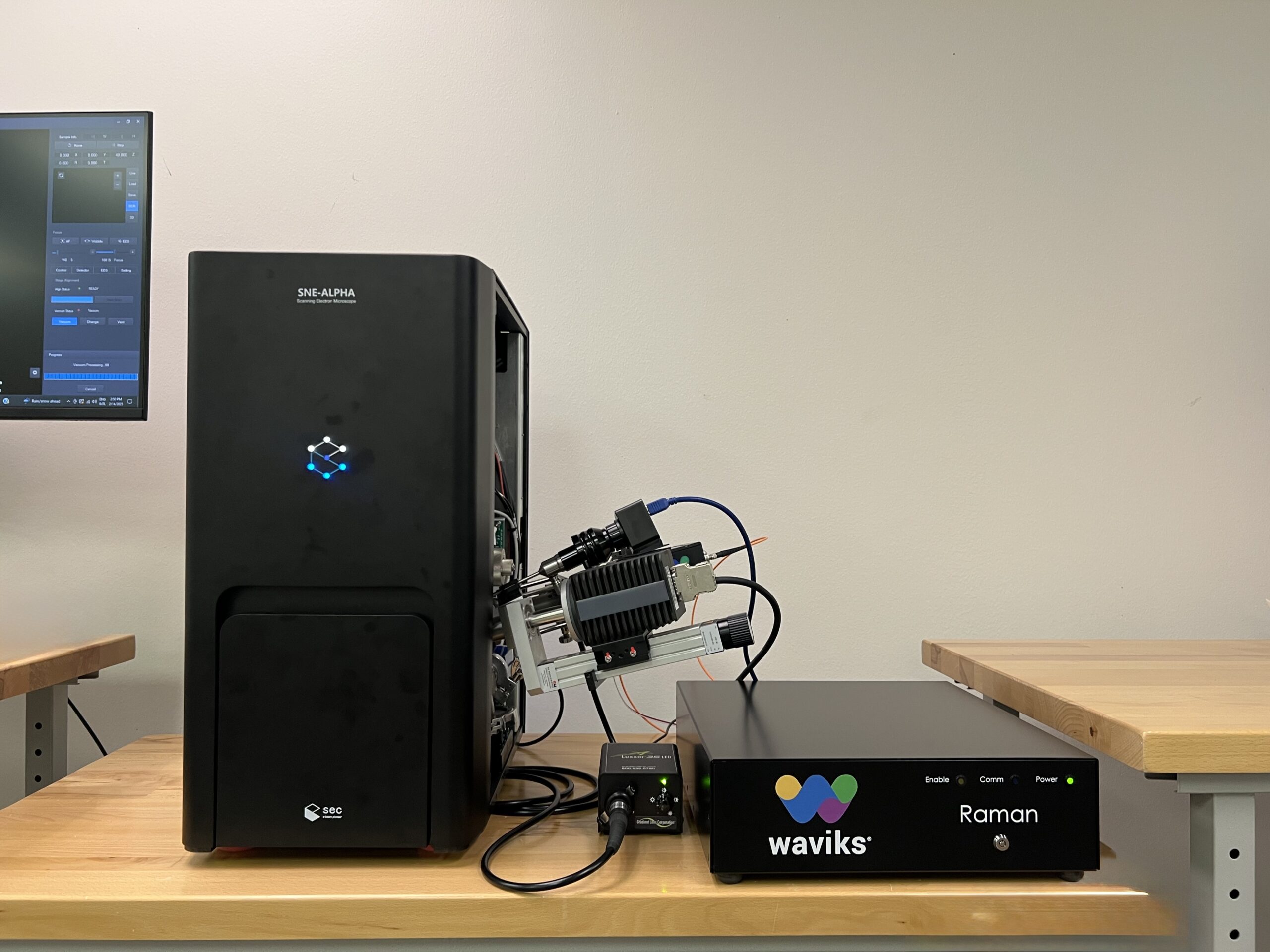
Cathodoluminescence (CL)
See the light your samples emit.
Cathodoluminescence detection reveals optical emission properties invisible to standard SEM detectors. Analyze defects in semiconductors, trace elements in minerals, and luminescence in biological samples with nanometer resolution.
See Cathodoluminescence in Action
Applications
Semiconductor Defects
Visualize dislocations, stacking faults, and recombination centers in GaN, GaAs, and other compound semiconductors.
Gemstone Analysis
Reveal growth zoning, defects, and treatments in diamonds and colored gemstones. Essential for gem certification.
Geology & Petrology
Image trace element distributions and growth textures in minerals. Understand geological processes and provenance.
Ceramics & Glasses
Characterize luminescent phases, rare earth dopants, and defect structures in ceramic and glass materials.
Applications
Materials Science
Metals, polymers, composites, failure analysis.
Life Sciences
Cells, tissues, biological structures.
Semiconductors
Wafer inspection, defect analysis, IC packaging.
Forensics
GSR analysis, trace evidence, fiber comparison.
Geosciences
Minerals, rocks, paleontology.
Nanomaterials
Nanoparticles, thin films, quantum dots.
Related Products
Resources
Reveal Hidden Optical Properties
CL provides information unavailable from any other SEM technique.
Discuss Your Application