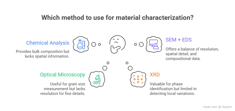
Alloys underpin high-performance applications in aerospace, automotive, energy, medical devices, and beyond. Before entering service, each batch must pass alloy qualification — a rigorous evaluation of chemical composition, microstructural consistency, and inclusion content against industry or customer specifications. These factors directly dictate mechanical behavior. Yet traditional bulk chemical techniques confirm nominal composition, but they cannot resolve where elements reside within the microstructure.
Scanning electron microscopy (SEM) paired with energy-dispersive spectroscopy (EDS) can resolve the issues of conventional analysis techniques. SEM provides nanoscale imaging of grains, precipitates, and inclusions, while EDS overlays spatially resolved chemistry. Together, they allow metallurgists to verify not just what is in the alloy, but how it is distributed — enabling faster, more reliable qualification.
What SEM + EDS Is and How It Works
Briefly: A scanning electron microscope (SEM) forms images by rastering a focused electron beam across the sample surface, generating signals such as secondary and backscattered electrons from interaction volumes only tens of nanometers in size. This allows resolution of grain boundaries, precipitates, and inclusions far below the optical limit. Imaging conditions—accelerating voltage, beam current, and working distance—can be tuned to emphasize either surface detail (e.g., low-kV imaging <5 kV for oxides or fine precipitates) or subsurface structure (higher kV for bulk features). Complementing this, energy-dispersive spectroscopy (EDS) detects characteristic X-rays emitted as atoms relax after electron displacement, producing spectra that quantify elemental composition.
Available Data Types
- Point Analysis: Localized spot measurements, useful for confirming the composition of inclusions, second-phase particles, or corrosion products. Spot size and interaction volume must be considered; at 20 kV the probed region may extend >1 µm into the bulk, so features smaller than this can yield mixed signals.
- Line Scans: Elemental profiles acquired along a user-defined path. Ideal for characterizing diffusion zones, weld interfaces, or segregation along grain boundaries. Step size and dwell time determine both spatial resolution and counting statistics.
- Area Mapping: Pixel-by-pixel X-ray acquisition across a region of interest. This produces compositional distribution maps, revealing gradients (e.g. carburization in steels), segregation in alloys, or contamination patterns. Modern systems can overlay EDS maps with SEM images for correlative analysis.
Why EDS Helps Accelerate Alloy Qualification
Integrating EDS into SEM workflows changes alloy characterization from a slow, centralized process into a rapid, localized one. Instead of waiting on wet chemistry or bulk spectroscopic techniques that require digestion, dissolution, or multiple preparation steps, SEM-EDS can directly interrogate polished cross-sections with minimal prep.
- Rapid Chemistry Screening: EDS provides near real-time spectra that confirm whether an alloy’s elemental composition meets specification. While not as precise as bulk ICP-OES or wet chemistry for trace quantification, the speed advantage makes it ideal for early-stage go/no-go checks.
- Phase and Inclusion Identification: Localized EDS spot analysis detects undesirable intermetallics, sulfide/oxide inclusions, or secondary precipitates that may compromise mechanical performance. Because the analysis is tied to SEM imaging, metallurgists can correlate microstructural context (e.g., grain boundaries, fracture surfaces) with chemistry in a single workflow.
- Segregation and Diffusion Insights: Compositional mapping across weld interfaces, heat-affected zones, or cast structures reveals elemental partitioning and microsegregation that drive brittleness, corrosion susceptibility, or phase instability. Line scans quantify diffusion profiles, enabling faster evaluation of heat-treatment or joining processes.
- Shorter Qualification Cycles: By delivering actionable data directly at the microscope, EDS eliminates the delays of outsourcing samples to a central analytical lab. Engineers can screen, qualify, or reject batches earlier in the production cycle, reducing scrap, rework, and downstream failures.
In effect, SEM-EDS provides both microstructural and chemical insight in the same session, collapsing what used to be multi-day workflows into hours. This acceleration is particularly valuable in industries like aerospace and automotive, where alloy qualification impacts yield, cost, and time-to-market.
Common Alloy Qualification Metrics via SEM + EDS
With the right setup, SEM + EDS provides valuable metrics that directly inform alloy approval:
- Inclusion Analysis: SEM imaging resolves inclusions down to the sub-micron scale, while EDS determines their chemistry (oxides, sulfides, nitrides, silicates). Automated particle analysis modules can generate size distributions, morphology statistics, and population densities across multiple fields of view. These metrics directly link to steel cleanliness, fatigue life, and machinability.
- Phase Identification: Secondary phases such as carbides, intermetallic compounds, or precipitates can be imaged and analyzed in situ. EDS spectra confirm elemental composition, while backscattered contrast highlights phase boundaries. This is critical for understanding precipitation hardening, embrittlement, or phase transformations induced by heat treatment.
- Grain Boundary Chemistry: Line scans or high-resolution mapping across grain boundaries reveal segregation of elements like P, S, or B that promote hot cracking, temper embrittlement, or intergranular corrosion. Unlike bulk analysis, SEM-EDS pinpoints the specific microstructural sites where these detrimental chemistries concentrate.
- Homogeneity Checks: Area mapping across polished cross-sections verifies that alloying additions (e.g., Cr, Ni, Mo, Ti) are evenly distributed. Localized depletion or clustering can flag incomplete mixing during casting or problems in secondary processing. This ensures that nominal bulk composition translates into consistent local properties.
By coupling structural imaging with localized chemistry, SEM-EDS provides a multidimensional dataset: not just what elements are present, but where they reside, in what phases, and how they interact with microstructural features that control performance.
Challenges and Best Practices
As with any analytical technique, SEM + EDS requires careful practice:
- Sample preparation artifacts (scratches, smearing) can obscure features.
- Overlapping spectral peaks may complicate elemental identification.
- Surface contamination or charging can distort signals.
- Statistical considerations are essential: a single inclusion is not representative; mapping larger areas improves reliability.
Recognizing these challenges ensures more robust alloy qualification outcomes.
Learn More—Analytical Scanning Electron Microscopy (SEM): Principles, Techniques, and Applications
Interested in New Solutions for Metallurgy Analysis?
SEM with EDS has transformed metallurgy analysis by providing rapid, detailed insight into alloy composition and structure. From inclusion analysis to segregation mapping, this combined approach accelerates qualification and supports more confident decision-making.
NanoImages delivers these capabilities through SEC’s SNE-Alpha tabletop SEM and Bruker QUANTAX ED-XS detectors, providing metallurgists with both imaging and elemental mapping in a compact, accessible system.
To see how SEM + EDS can enhance your alloy qualification processes, contact NanoImages today to request a demo or trial analysis.