
Micro-Electronics
Circuit inspection, solder joints, wire bonding, and electronic component analysis
The micro-electronics industry demands precise inspection at ever-smaller scales. As components shrink and integration densities increase, scanning electron microscopy becomes essential for quality control, failure analysis, and process development in semiconductor and electronics manufacturing.
The SNE-Alpha desktop SEM provides micro-electronics labs with high-resolution imaging capability without the complexity of floor-model systems. Its compact footprint fits easily into cleanroom environments, while the intuitive operation enables rapid inspection of production samples and failure analysis specimens.
Key Micro-Electronics Applications
- Solder Joint Inspection: Examine solder ball morphology, intermetallic formation, and joint defects in BGA, flip-chip, and through-hole assemblies
- Wire Bonding Analysis: Inspect ball bonds, wedge bonds, and wire-to-pad adhesion for quality control and failure investigation
- PCB Inspection: Examine via structures, trace integrity, and plating quality on printed circuit boards
- Component Defects: Identify cracks, voids, delamination, and contamination in passive and active components
- Die Surface Analysis: Inspect semiconductor die surfaces for scratches, particles, and process defects
- Connector Inspection: Analyze contact surfaces, plating wear, and corrosion in electrical connectors
Failure Analysis Support
SEM is a cornerstone technique for electronics failure analysis:
- Root Cause Investigation: Identify failure modes in returned products and field failures
- EOS/ESD Damage: Characterize electrical overstress and electrostatic discharge damage
- Corrosion Analysis: Examine corrosion products and identify contamination sources with EDS
- Mechanical Failure: Analyze fracture surfaces and stress-induced damage
Micro-Electronics SEM Images
Sample images captured with the SNE-Alpha desktop SEM.
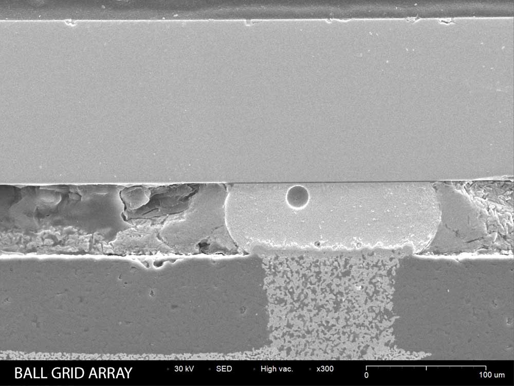
BGA Solder Balls
Ball grid array solder ball inspection

Wire Bonding
Gold wire bond connection analysis

IC Cross-Section
Semiconductor chip internal structure analysis

Bond Pad
IC bond pad surface inspection

Wafer Structure
Semiconductor wafer surface detail
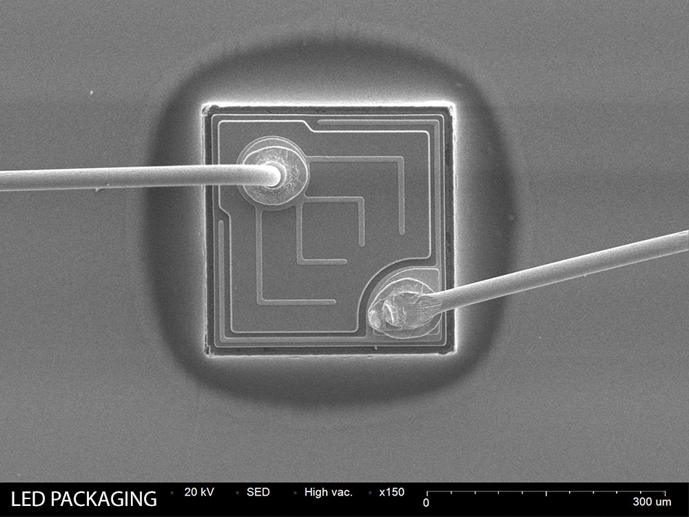
LED Packaging
LED device packaging and wire bond inspection
Industry Applications
SMT Assembly
Inspect solder paste deposits, reflow profiles, and component placement in surface mount manufacturing.
Semiconductor Packaging
Analyze wire bonds, die attach, and package integrity in IC assembly operations.
PCB Manufacturing
Evaluate via plating, trace etching, and solder mask quality in board fabrication.
Reliability Testing
Support accelerated life testing with pre- and post-test inspection of test vehicles.
Recommended Equipment
SNE-Alpha Desktop SEM
Compact, high-resolution scanning electron microscope ideal for research and quality control applications.
Bruker XFlash EDS
Energy dispersive X-ray spectroscopy for elemental analysis and material identification.
MCM-100 Sputter Coater
Prepare non-conductive samples with gold or platinum coatings for optimal SEM imaging.
Related Applications
Resources
Electronics Analysis Solutions
See how the SNE-Alpha can support your micro-electronics inspection and failure analysis needs.
Request Sample Analysis