There has never been a tabletop SEM that could do what this one does.
Elemental analysis. Crystallographic mapping. Molecular fingerprinting. All on the same sample, in the same vacuum, at the same coordinate, on a benchtop instrument. Until now, that capability set lived in floor-model microscopes — instruments that need a dedicated room, three-phase power, vibration isolation, and a budget well north of half a million dollars before you’ve fitted a single detector.
We’re putting it on a bench, and we’re putting it in the hands of researchers who shouldn’t have to choose between throughput and analytical depth.
The configuration pairs the SEC SNE-Alpha desktop SEM with a Bruker QUANTAX EDS detector, Bruker’s eFlash XS EBSD detector, and the Waviks Vesta™ Raman spectrometer — all on a single column, all controlled from a single workspace, all addressing the same spot on the same sample. No
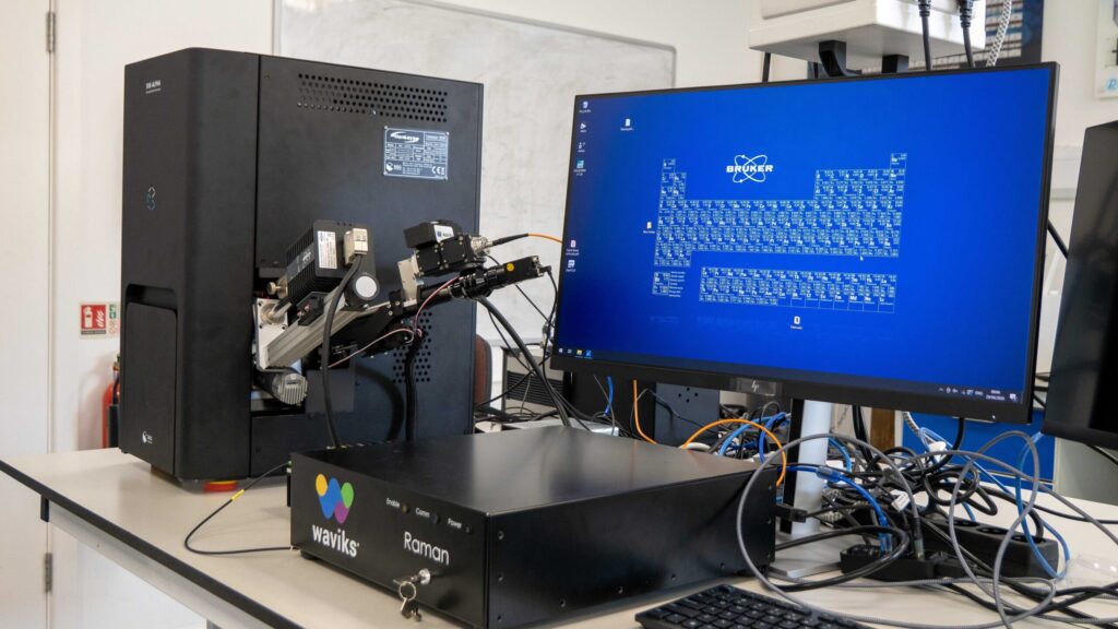
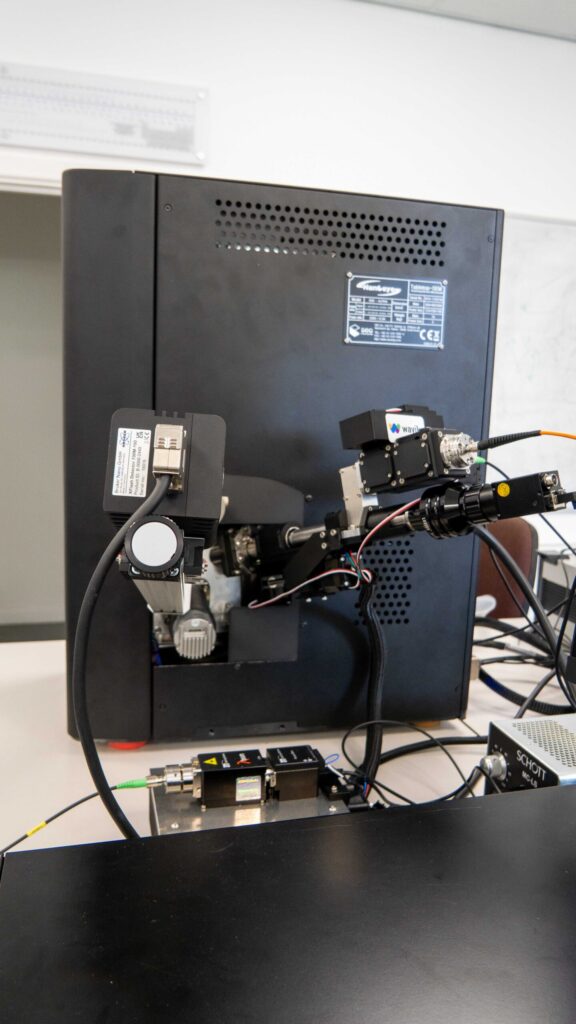
transfer. No re-registration. No sequential workflow across separate instruments.
Why In-Situ Multimodal Analysis Actually Matters
Anyone who has spent time chasing a feature across multiple instruments knows the problem. You image a particle on the SEM. You think you’ve found what you need. Then the sample goes to the Raman bench, where you can no longer see the BSE contrast that told you where to look. By the time you’ve reacquired position — assuming you can — you’ve lost hours, possibly the particle itself.
In-situ multimodal analysis eliminates the transfer. The electron beam, the X-ray detector, the EBSD camera, and the Raman laser all converge on the same eucentric point. The sample sees one vacuum cycle, one stage coordinate system, one operator session.
For beam-sensitive materials — pharmaceuticals, polymers, biologicals — that’s not a convenience improvement. It’s the difference between getting the measurement and not.
Three Analytical Pillars on a Single SEM Column
High-Resolution SEM Imaging
The SNE-Alpha tabletop SEM delivers 5 nm SE resolution at 30 kV across a full 1–30 kV accelerating range, with a 5-axis motorized stage that tilts from −45° to 90°. The column geometry is pre-engineered with factory-ready ports for every analytical add-on, which is the only reason this integration is possible at all. The base instrument is manufactured by SEC Co. Ltd. of Suwon, South Korea, and distributed exclusively in the US by NanoImages.
EDS Elemental Analysis
The Bruker XFlash® 630 silicon drift detector covers Boron to Uranium, with the energy resolution and throughput needed for both point analysis and full-field elemental mapping. No liquid nitrogen required. Bruker’s ESPRIT Compact software handles acquisition, quantification, and reporting.
EBSD Crystallographic Mapping
Bruker’s eFlash XS EBSD detector — the EBSD half of the QUANTAX ED-XS package — adds phase identification, grain orientation mapping, and texture analysis under the same ESPRIT software environment as the EDS. EDS and EBSD data are acquired together and indexed together. For metallurgy, welds, additively manufactured parts, and any material where grain boundaries dictate failure, this is the workhorse pairing.
In-Chamber Raman Spectroscopy
The Waviks Vesta™ integrates Raman spectroscopy through a custom flange that places the laser and collection optics in the chamber at a fixed working distance. A single-mode laser delivers a sub-10 µm probe to the same point the electron beam is interrogating. The Raman spectrum identifies polymers, polymorphs, carbon allotropes, minerals — anything with a vibrational fingerprint — and overlays it onto the SEM image and EDS map without any operator hand-registration.
Applications: What This Configuration Unlocks
The combination is more than the sum of its parts. A few examples from our applications lab:
Pharmaceutical Polymorphism
Two crystal forms of the same active ingredient can be indistinguishable in SEM and identical in EDS. Raman tells them apart in seconds. EDS-classify the population, then Raman-fingerprint only the suspects. The entire screen happens without venting the chamber.
Forensic Gunshot Residue Analysis
The accepted SEM/EDS workflow identifies the lead-barium-antimony signature of inorganic primer residue. Raman adds the organic propellant chemistry — nitrocellulose, stabilizers, oxidizers — on the same particle, in the same instrument, in one report.
Failure Analysis of Welds and Metals
Welded joints, rolled steels, and additively manufactured parts fail at grain boundaries. EBSD maps the boundary geometry; EDS catches the segregated impurities; Raman picks up oxide phases that EDS alone can’t disambiguate. All on the fracture surface, no remounting.
Battery and Energy Materials Characterization
Cathode particles need elemental mapping (Bruker’s strength), crystal phase distribution (EBSD), and SEI chemistry (Raman). This configuration is the only tabletop platform on the market that delivers all three on the same particle in the same session.
Geosciences and Mineralogy
Mineral identification has historically required hand-off between three benches: SEM for morphology, electron microprobe or EDS for chemistry, and a benchtop Raman for confirmation of polymorphs like calcite versus aragonite, or anatase versus rutile. On this platform, the analyst stays in one workspace. Trace inclusions in a host mineral get imaged, elementally fingerprinted, and Raman-confirmed without losing the spatial context that makes the analysis meaningful.
One Workspace, One Operator
The integration goes deeper than co-locating detectors. ESPRIT runs EDS and EBSD as a unified acquisition, with shared coordinates and combined indexing. Waviks’ Vesta software exposes a Python SDK and Ethernet control, so the Raman acquisition can be triggered from the same session-level workflow that drives the SEM stage and the X-ray detector.
An operator who knows the SEM can run all three modalities without learning three separate software stacks — a difference that matters in any lab where the people doing the analysis aren’t full-time microscopists.
What This Means for the Tabletop SEM Market
Tabletop SEM has historically meant a compromise: lower cost, smaller footprint, fewer detectors. The SNE-Alpha breaks that compromise. Compare it to the other desktop SEMs available in 2026 — Phenom, Hitachi TM-series, JEOL JCM — and the integration story is unique. Phenom offers a proprietary EDS. Hitachi and JEOL support third-party EDS. None of them offers EBSD plus Raman, in-situ, in this form factor.
Floor-model SEMs can be configured this way. They start at four to five times the price and require facility infrastructure most labs simply don’t have.
For the researcher who’s been told they need to buy three instruments to characterize one sample, that math just changed.
Available Now
Configurations are quoted on a per-application basis. If you’re evaluating analytical SEM capability — replacing an aging floor system, expanding a teaching lab, or standing up a new characterization facility — we’ll work through the use case with you and propose the right integration. The base SNE-Alpha is in stock, and the analytical add-ons integrate factory-aligned at delivery.
Send us your samples. We’ll show you what one column can do.